Preprint: Revealing the Atomic Structure of NiO/Ga₂O₃ Interfaces
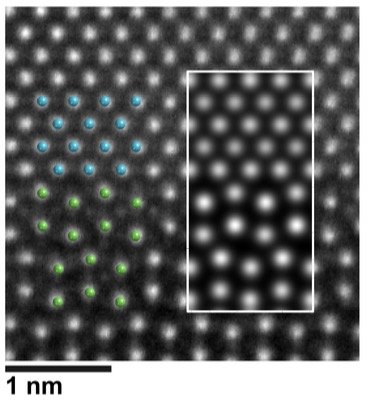
Heterojunctions combining NiO and β-Ga₂O₃ have drawn sustained attention for power electronics, owing to the ultrawide bandgap and wafer-scale availability of Ga₂O₃ alongside the controllable p-type doping achievable in NiO. While the community has made significant progress in understanding crystallinity, carrier transport, and band structure in these heterojunctions, the atomic-scale structure of the interface itself — the boundary where Ga₂O₃'s monoclinic lattice meets NiO's cubic structure — has remained comparatively underexplored. This gap matters: interface atomic positions and bonding environments strongly influence band alignment, phonon transport, and the trap states that govern device performance and long-term stability.
In this work, led by Michelle Smeaton, we directly visualize and compare NiO/Ga₂O₃ interface structure across three substrate orientations — (100), (2̄01), and (001) — using aberration-corrected scanning transmission electron microscopy in combination with interface modeling and image simulation. Michelle's high-resolution STEM imaging, paired with careful simulation work to disentangle genuine atomic-scale structure from the 3D-to-2D projection effects inherent to thin-specimen imaging, provides the clearest picture yet of how these interfaces actually form.
The results are clarifying. NiO/Ga₂O₃ (100) exhibits sharp crystallographic registry and limited structural variation relative to the (2̄01) and (001) orientations, consistent with fewer nucleation sites for NiGa₂O₄ interlayer phase formation during high-temperature device operation. The (2̄01) interface reveals a "corrugated" Ga₂O₃ surface introducing added atomic positions not fully captured by interface calculations, while the (001) interface proves the most structurally complex, with a near-(331) tilted NiO growth orientation. Collectively, these findings support increased focus on (100)-oriented Ga₂O₃ as a candidate substrate for fabricating high-quality, low-defect-density NiO/Ga₂O₃ heterojunction devices, while underscoring that interpretation of STEM contrast at any of these interfaces requires careful accounting for specimen thickness and projection effects — a consideration that will be essential as the field moves toward understanding interface stability under real device operating conditions.
This work was carried out by Michelle A. Smeaton, Krishna Acharya, Anna Sacchi, Renae N. Gannon, M. Brooks Tellekamp, Andriy Zakutayev, Vladan Stevanović, and Steven R. Spurgeon, and was supported by the APEX (A Center for Power Electronics Materials and Manufacturing Exploration) Energy Frontier Research Center, funded by the U.S. Department of Energy, Office of Science, Basic Energy Sciences.